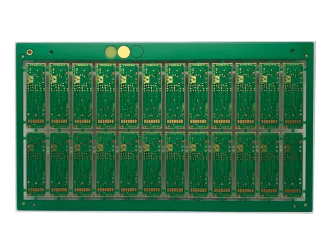
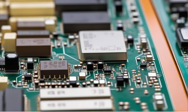
The Best PCB Prototyping Machines:Top Solutions from Victory in 2025
When it comes to PCB prototyping, selecting the right solution can make all the difference in bringing your electronic designs to life….
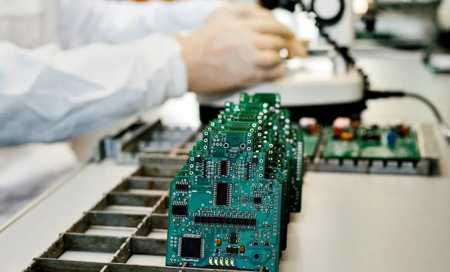
Shenzhen Victory Electronic Technology Co., Ltd is located in beautiful Shenzhen, Guangdong province, China where there are very rich supply chains and resources. We design, research and develop all kinds of 1-6layer flex PCB, PCB Assembly and 1-32layer rigid PCB.
When it comes to PCB prototyping, selecting the right solution can make all the difference in bringing your electronic designs to life….
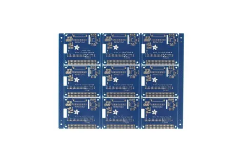
Double-sided PCB, Multilayer PCB, Aluminum PCB, and Flexible PCB. Each is highlighted for its unique advantages, supported by technical specifications and customer feedback. The Double-sided PCB excels in compact, efficient designs; the Multilayer PCB is ideal for high-density, high-frequency applications; the Aluminum PCB offers superior thermal management; and the Flexible PCB provides unmatched versatility for dynamic uses. Tailored for hobbyists, engineers, and industrial professionals, these PCBs cater to diverse needs, from power supplies to wearable technology, showcasing Victory’s expertise in delivering high-quality fabrication solutions.

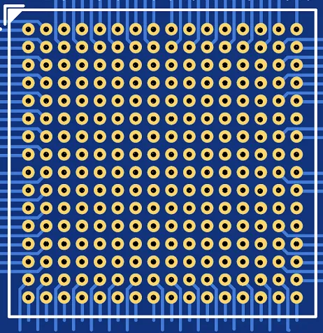
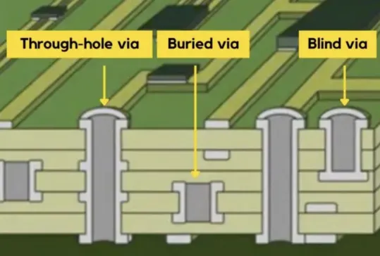
HDI PCB (High-Density Interconnect PCB) is a cutting-edge technology used to create compact and complex electronic circuits with extremely high connection densities. Featuring microvias, fine-pitch traces, and sequential lamination, HDI PCBs are crucial in applications where space is limited, such as smartphones, medical implants, and advanced automotive systems. These circuit boards offer superior signal integrity, minimal signal loss, and enhanced thermal management, making them ideal for high-speed and high-frequency devices like 5G communication systems. This article dives into the essential features of HDI PCBs, such as stacked, staggered, and skip vias, their role in 5G devices, and the advanced testing methods like Automated Optical Inspection (AOI) used to ensure quality and reliability in production. Explore why HDI PCBs are shaping the future of electronics and their critical importance in today’s high-performance devices.
Printed circuit boards (PCBs) are vital for electronics. The PCB substrate material affects performance and application suitability. Rogers PCB vs FR4 PCB…
Victory is a trusted PCB fabrication company with years of experience providing quality PCB solutions. As a leading PCB company, we understand…
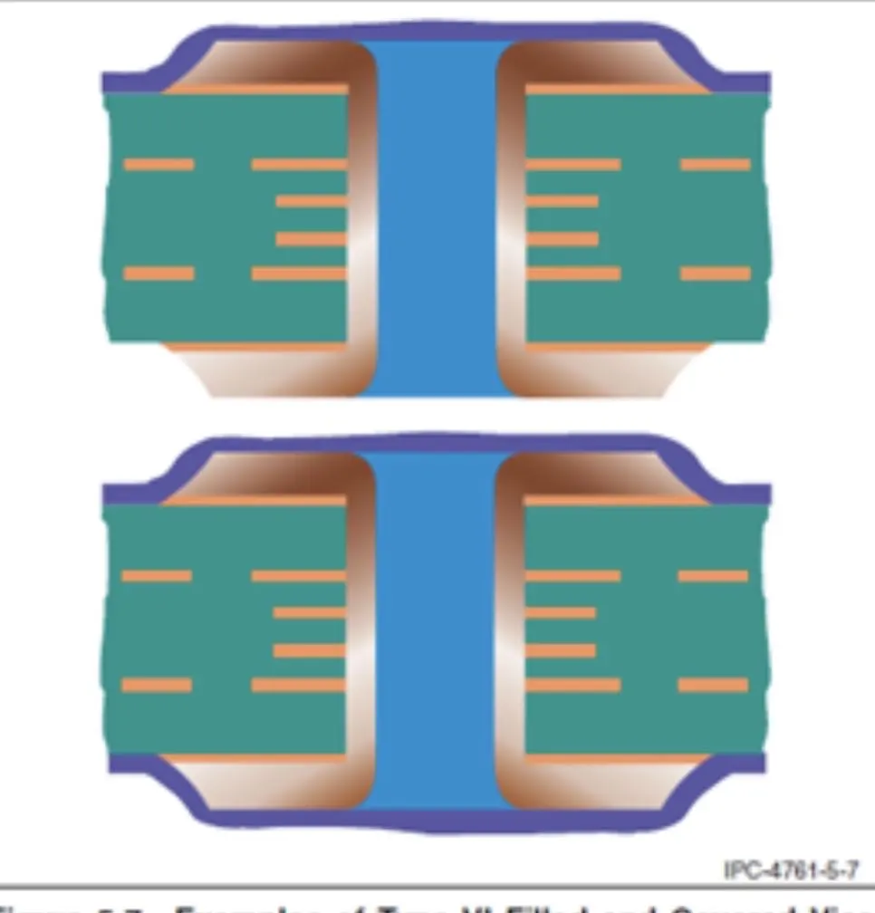
When designing a printed circuit board (PCB), selecting the right interconnection methods is critical for effective implementation. Two common interconnects are plated…
Printed circuit boards (PCBs) are vital for electronics.Printed circuit boards can be divided into single-layer boards and multi-layer boards As designs evolve,…
Selecting the optimal copper weight is a crucial decision in PCB design. Copper weight, typically measured in ounces per square foot (oz),…
Multilayer PCBs have become indispensable components in contemporary electronic devices. As electronic technologies advance, devices are gaining greater sophistication and requiring denser,…
PCB is closely related to our lives,designing the layer stackup for a printed circuit board (PCB) involves many constraints. High-speed designs require…