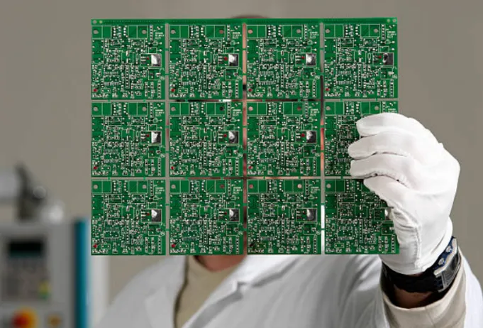
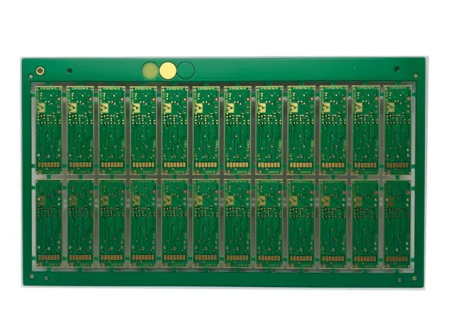
1. What is HDI PCB?
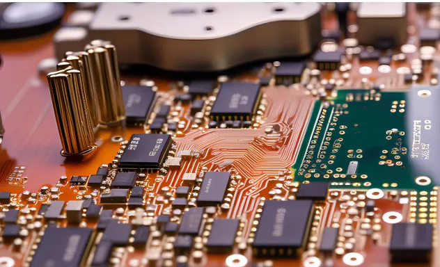
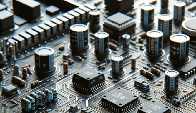
HDI (High-Density Interconnect) PCBs are advanced circuit boards designed to accommodate complex electronics in compact spaces. Unlike traditional PCBs, HDI technology uses microvias (laser-drilled holes <150μm), fine-pitch traces (line width/spacing ≤75μm), and sequential lamination to achieve wiring densities exceeding 20,000 connections per square inch.
Key Structural Features:
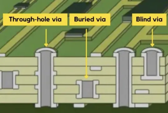
- Blind/Buried Vias: Reduce layer transitions by connecting adjacent layers without penetrating the entire board.
- Thin Dielectrics: Materials like Megtron 6 or Isola 370HR with Dk ≤3.5 for signal integrity.
- Via-in-Pad: Directly places vias under component pads to save space.
Applications:
- Smartphones (e.g., iPhone 15’s 10-layer HDI stackup).
- Medical implants (pacemakers with 0.4mm pitch components).
- Automotive ADAS systems (Tesla’s Autopilot modules).
2. What Are Stacked, Staggered, and Skip Vias in HDI PCB?
Stacked Vias:
Vertical alignment of microvias across multiple layers.
- Use Case: High-speed DDR5 memory routing.
- Limitation: Requires precise laser drilling (±25μm tolerance).
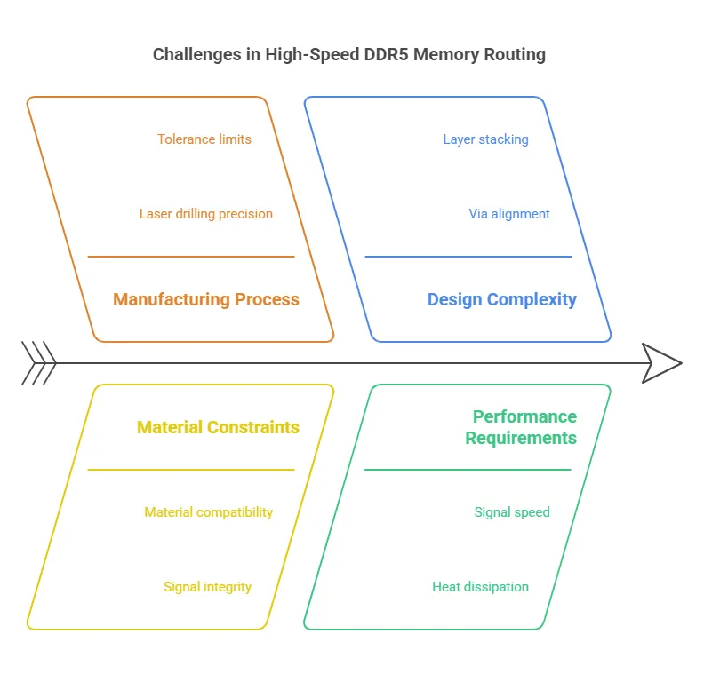
Staggered Vias:
Offset microvias between layers to reduce stress concentration.
- Advantage: Improves thermal reliability by 30% (IPC-6012E).
- Design Rule: Minimum 150μm spacing between adjacent vias.
Skip Vias:
Microvias that “skip” intermediate layers to connect non-adjacent layers.
- Application: RF front-end modules in 5G base stations.
- Risk: Increased capacitance if anti-pad clearance <100μm.
3. Why HDI PCB is Essential for 5G Communication Devices
5G mmWave frequencies (24–40GHz) demand:
- Low Signal Loss: HDI’s ultra-low roughness copper (≤0.5μm Ra) minimizes skin effect losses.
- Impedance Control: Tight ±5% tolerance using hybrid Rogers/FR-4 materials.
- Thermal Management: 2W/m·K thermal conductive substrates (e.g., Arlon 85N) for power amplifiers.
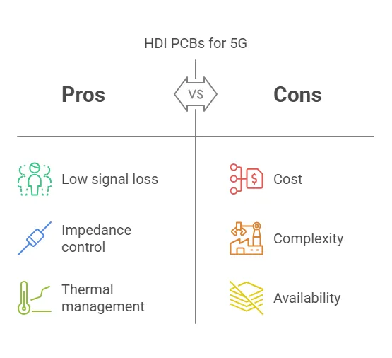
Real-World Impact:
- Ericsson’s 5G mMIMO radios use 14-layer HDI PCBs to achieve 64T64R antenna arrays.
- Failure to adopt HDI results in 15–20% slower data rates (Qualcomm 2023 whitepaper).
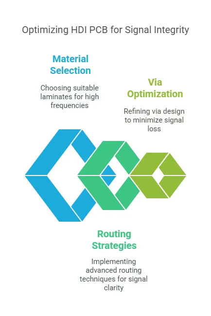
4. How HDI PCB Improves Signal Integrity in High-Frequency Applications
Step-by-Step Optimization:
-
Material Selection:
- Choose laminates with Df ≤0.002 at 10GHz (e.g., Panasonic Megtron 7).
- Avoid FR-4 for frequencies >5GHz.
-
Routing Strategies:
- Implement differential pairs with length matching ≤50μm.
- Use ground-shielded traces for 28GHz+ signals.
-
Via Optimization:
- Back-drill unused via stubs >85% (critical for PCIe 6.0).
- Apply via tenting with soldermask to reduce capacitance.
Measurable Results:
- 40% lower crosstalk in 25Gbps SerDes links.
- 0.5dB insertion loss reduction at 28GHz.
5. What is AOI (Automated Optical Inspection) in HDI PCB Manufacturing?
AOI systems use 10MP cameras and AI algorithms to detect defects in HDI boards:
Critical Inspection Points:
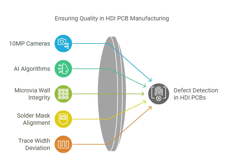
- Microvia Wall Integrity: Cracks >10μm flagged (per IPC-A-600).
- Solder Mask Alignment: Tolerance ±35μm.
- Trace Width Deviation: >±15% from design rejected.
AOI Workflow:
- Pre-Lamination Scan: Checks inner layer registration.
- Post-Etching Scan: Verifies 75μm trace accuracy.
- Final Inspection: 3D height mapping for BGA coplanarity.
Industry Data:
- AOI reduces HDI scrap rates from 8% to <1.2% (Shennan Circuits 2024 report).
- False call rate <0.3% with deep learning models.