Double-sided PCB
| P/N: Q2P06438A0 | Layer Count: 2L | Min Line W/S: 8/8mil |
| Material: FR-4 Tg 130 | Cu Thickness: 1oz | Min PTH: 0.4mm |
| Board Thickness: 0. 5mm | Surface: ENIG | Application: Automotive |
| Soldermask Color: Green | Board Size: 171.00mmX170.00mm(1-up) | |
| Others: IPC-A-600 Class 3 | ||
Knowledge of double-sided PCBs
Double-sided PCB which both sides are covered with copper and traces and vias can be used to connect the circuits between the two layers to connect the required network. Double-sided PCB can deal with the difficulty of interlaced circuit in single-sided PCB,so it is more suitable to use on more complex circuits than single-sided PCB.
Advantages of double-sided PCBs
Advantages (compared to single-sided boards): convenient,simple wiring,shorter line lengths and so on.
Design operation steps of double-sided PCBs
- Prepare the circuit drawings
- Make a new pcb gerber and load it into the component package
- Programme the circuit
- Place net-list and components
- Automatic layout of components
- Layout adjustment
- Network density analysis
- Set wiring rule
- Automatic routing
- Manual adjustment of routing
What is Double-sided PCB?
A double-sided PCB, or double-sided printed circuit board, is a type of PCB that features conductive copper traces on both the top and bottom layers of the board. Unlike single-sided PCBs, which only have conductive material on one side, double-sided PCBs allow for more complex circuit designs by utilizing both sides of the board. This design enables components to be mounted on either side, increasing the density of the circuit and making it more versatile for various applications. Double-sided PCBs are distinct from multi-layer PCBs, which have additional internal layers of conductive material, as they only utilize two layers.
Why Use Double-sided PCBs?
Double-sided PCBs are widely used because they offer a balance between complexity and cost. They provide more routing options compared to single-sided PCBs, making them suitable for more intricate circuits without the added expense of multi-layer PCBs. Their ability to accommodate components on both sides makes them ideal for compact designs, which is particularly useful in modern electronics where space is often limited. Additionally, double-sided PCBs are easier to manufacture than multi-layer boards, making them a cost-effective solution for many applications.
What is the Structure of a Double-sided PCB?
The structure of a double-sided PCB consists of several key elements:
- Top and Bottom Copper Layers: These are the conductive layers where the circuit traces are etched. Components are mounted on both sides.
- Substrate Material: Typically made of fiberglass (FR-4), this insulating layer provides structural support and separates the two copper layers.
- Vias: These are small holes drilled through the board and plated with conductive material to connect the top and bottom layers.
- Solder Mask: A protective layer applied over the copper traces to prevent short circuits and oxidation.
- Silkscreen: Used for labeling components, test points, and other important information on the board.
What are the Applications of Double-sided PCBs?
Double-sided PCBs are used in a wide range of industries and devices due to their versatility and efficiency. Some common applications include:
- Telecommunications: Used in devices like routers, modems, and communication modules.
- Automotive: Found in control systems, sensors, and entertainment systems.
- Medical Devices: Used in diagnostic equipment, monitoring systems, and imaging devices.
- Consumer Electronics: Found in smartphones, tablets, and home appliances.
- Industrial Equipment: Used in power supplies, control systems, and automation equipment.
Can Double-sided PCBs Be Used in High-Frequency Applications?
Yes, double-sided PCBs can be used in high-frequency applications, but careful design considerations are necessary. High-frequency signals are more susceptible to interference and signal loss, so the layout of the traces, the choice of materials, and the placement of components must be optimized. Techniques such as controlled impedance routing, proper grounding, and the use of high-quality dielectric materials can help ensure reliable performance in high-frequency applications.
What Are the Key Design Considerations for Double-sided PCBs?
Designing a double-sided PCB requires careful planning to ensure optimal performance and manufacturability. Key factors to consider include:
- Component Placement: Components should be strategically placed to minimize signal interference and ensure efficient routing. High-speed or sensitive components may need to be isolated from noisy ones.
- Layer Routing: Traces on both layers must be routed to avoid crossing or overlapping, which can cause signal interference. Proper spacing and trace width are critical for signal integrity.
- Via Technology: Vias are essential for connecting traces between layers. Consider using through-hole vias, blind vias, or buried vias depending on the complexity of the design.
- Thermal Management: Heat-generating components should be placed to allow proper heat dissipation, and thermal vias can be used to transfer heat to the opposite layer.
- Signal Integrity: High-frequency signals require controlled impedance routing and proper grounding to minimize noise and signal loss.
Why Are Double-sided PCBs Advantageous?
Double-sided PCBs offer several advantages over single-sided PCBs, making them a popular choice for many applications:
- Compact Size: By utilizing both sides of the board, double-sided PCBs allow for higher component density, making them ideal for compact devices.
- Cost-Effectiveness: They are more affordable than multi-layer PCBs while offering greater design flexibility than single-sided boards.
- Complex Circuit Handling: Double-sided PCBs can accommodate more complex circuits, making them suitable for advanced applications.
- Improved Performance: With proper design, they can support higher signal speeds and better thermal management.
- Versatility: They are used across various industries, from consumer electronics to industrial automation.
How to Choose Materials for Double-sided PCBs?
The materials used in double-sided PCBs play a critical role in their performance and durability. Common materials include:
- Substrate Material: FR-4 is the most widely used substrate due to its excellent mechanical and electrical properties. For high-frequency applications, materials like Rogers or Teflon may be used.
- Copper Layers: The thickness of the copper layer (measured in ounces per square foot) affects current-carrying capacity and heat dissipation. Common thicknesses include 1 oz and 2 oz.
- Solder Mask: This protective layer prevents short circuits and oxidation. It is available in various colors, with green being the most common.
- Silkscreen: Used for labeling, it is typically made of epoxy-based ink.
What Soldering Techniques Are Used for Double-sided PCBs?
Soldering double-sided PCBs requires specialized techniques to ensure reliable connections on both sides:
- Wave Soldering: This method is used for through-hole components. The board passes over a wave of molten solder, which attaches to the exposed metal areas.
- Reflow Soldering: Commonly used for surface-mount components, this technique involves applying solder paste and heating the board in a reflow oven.
- Hand Soldering: For prototyping or repairs, hand soldering with a soldering iron is used. It requires precision to avoid damaging components or creating solder bridges.
Challenges and Solutions: Soldering double-sided PCBs can lead to issues like tombstoning or solder bridging. Proper temperature control, solder paste application, and component placement can mitigate these problems.
How Are Double-sided PCBs Tested and Inspected?
Testing and inspection are critical to ensuring the quality and reliability of double-sided PCBs. Common methods include:
- Electrical Testing: Conductivity tests are performed to verify that all connections are properly made and there are no open or short circuits.
- Visual Inspection: Manual or automated inspection is used to check for defects like misaligned components, solder bridges, or missing parts.
- Automated Optical Inspection (AOI): Cameras and software are used to detect surface-level defects, such as incorrect component placement or soldering issues.
- X-ray Inspection: This method is used to inspect hidden connections, such as those under ball grid array (BGA) components or within vias.
- Functional Testing: The PCB is tested under real operating conditions to ensure it performs as intended.
By following these testing and inspection procedures, manufacturers can ensure that double-sided PCBs meet the required standards for quality and reliability.
Applications of double-sided PCBs
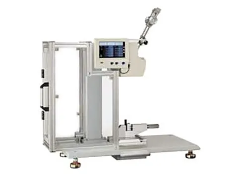
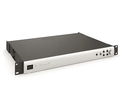
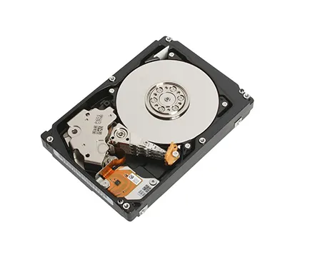
Double-sided PCB can be used widely in various fields and has range of applications:
∗ Hard drives ∗ Car dashboards ∗ Traffic systems
∗ Converters ∗ Vending machines ∗ Amplifiers
∗ UPS power system ∗ Power monitoring ∗ Control relays
∗ Automotive dashboards ∗ Power conversion ∗ Test equipment
Our product display


FAQ
Reviews