HDI PCB
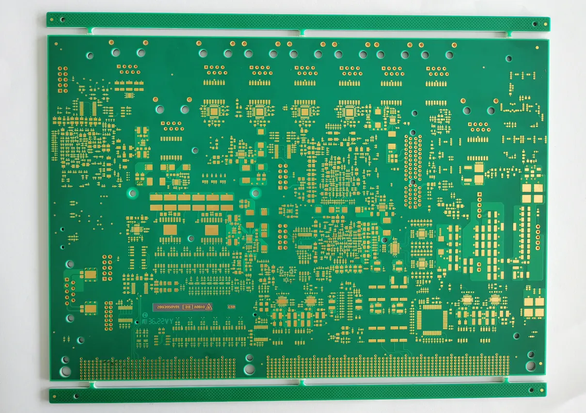
| P/N: S8l1 7966A0 | Layer Count: 8L | Min Line W/S: 4/4mil |
| Material: IT180. | Cu Thickness: 1/0.5oz | Min PTH: 0.1mm |
| Board Thickness: 1. 6mm | Surface: ENIG | Application:Industry Control |
| Soldermask Color: Blue | Board Size: 164.00mmX146. 30mm | |
Product Features
What is HDI PCB
HDI : High Density Interconnection Technology.
Non mechanical drilling, micro blind hole size less than or equal to 150um (6mil), the trace L/S between inner and outer layers less than 4mil, pad diameter ≤ φ The 0.35mm increase layer method for multi-layer board production is called HDI board
Compact design
The combination of micro vias, blind vias, and buried vias greatly reduces board space. With the support of HDI technology, a standard 8-layer through-hole PCB can be simplified into a 4-layer HDI PCB but with the same functions.
Excellent signal integrity
With smaller vias than normal PCBs, all stray capacitance and inductance will be reduced. Combining the technology of bonding vias and vias in pads helps to shorten the length of the signal path. These will lead to faster signal transmission and better signal quality.
High reliability
HDI technology easier wiring and connection, and provides PCBs with better durability and reliability under hazardous conditions and extreme environments.
Save costs
If the traditional pressing process is used and the board layer exceeds 8 layers, then more manufacturing costs are required. But HDI technology can reduce costs and maintain functional purpose.
Products application

HDI is currently widely used in mobile phones, digital (camera) cameras, MP3, MP4, notebook computers, automotive electronics and other digital products like medical equipment, among which mobile phones are the most widely used. HDI boards are generally manufactured by the build-up method. The more layers are built up, the higher the technical grade of the board. Ordinary HDI boards are basically one-time build-up, and high-end HDI uses two or more build-up technologies, and at the same time adopts advanced PCB technologies such as stacked holes, electroplating and filling holes, and laser direct drilling. HDI multi-layer circuit board production.
- Mobile Phone
- Digital Products
- Notebook Computers
- Automotive Electronics
- Medical Equipment
Industry information
The development of HDI PCB technology has brought unprecedented design freedom and flexibility to engineers, allowing more components to be placed on both sides of the original PCB as needed, while allowing smaller components to be placed together. This means that HDIPCB ultimately results in faster signal transmission as well as enhanced signal quality.
HDI PCBs are widely used to reduce the weight and overall size of products, as well as enhance the electrical performance of devices; often appear in mobile phones, touch screen devices, laptops, digital cameras and 4G network communications. HDI PCBs are also prominent in medical equipment as well as various electronic aircraft components.
Most High Density PCB have small tracks width and gap min. 3/3mil, which let engineers realize more functions on one limited dimension PCB.
Shall you have any inquiry about HDI PCB, pls feel free to contact with us.
What is an HDI PCB?
An HDI PCB, or High-Density Interconnect Printed Circuit Board, is an advanced type of circuit board designed for compact, high-performance electronics. It features finer traces, smaller vias, and higher connection density than traditional PCBs, allowing more components to fit in a smaller space. Built with microvias and multiple layers, HDI PCBs are the backbone of modern devices like smartphones, tablets, and medical equipment, delivering speed and efficiency in miniature designs.
How Are HDI PCBs Manufactured?
The manufacturing of HDI PCBs is a precise, multi-step process tailored for high density:
- Design Planning: Engineers create layouts with tight spacing and microvias.
- Layer Build-Up: Stack thin layers of substrate, bonding them with adhesives.
- Microvia Drilling: Use lasers to create tiny, precise holes for connections.
- Copper Plating: Coat vias and traces to ensure conductivity.
- Final Assembly: Add solder masks and test the board’s integrity.
This process enables the creation of intricate, reliable boards for cutting-edge technology.
How Does an HDI PCB Work?
An HDI PCB operates by routing electrical signals through densely packed traces and microvias across multiple layers. The smaller vias reduce signal travel distance, boosting speed and reducing latency. Components are surface-mounted with precision, and the board’s layered structure supports complex circuits in a compact footprint. This design ensures efficient power distribution and signal clarity, critical for high-performance devices.
Where Are HDI PCBs Used?
HDI PCBs are integral to industries requiring miniaturized, high-speed electronics:
- Consumer Tech: Powers slim devices like laptops and wearables.
- Medical: Drives compact diagnostic tools and implants.
- Automotive: Supports advanced driver-assistance systems (ADAS).
- Telecom: Enhances 5G equipment with dense circuitry.
Their small size and big capabilities make them a staple in modern innovation.
Why Choose HDI PCBs?
HDI PCBs offer compelling advantages for advanced electronics:
- Space Efficiency: Packs more tech into smaller areas.
- Faster Signals: Shortens paths for quicker data transfer.
- Reliability: Reduces connectors, boosting durability.
- Versatility: Fits complex designs with ease.
These benefits make HDI PCBs ideal for next-gen devices demanding performance and compactness.
What Design Factors Shape HDI PCBs?
Designing an HDI PCB requires attention to detail:
- Trace Width: Narrower traces maximize density.
- Microvias: Smaller, laser-drilled vias save space.
- Layer Count: More layers handle complex circuits.
- Material Choice: High-quality laminates ensure signal stability.
These considerations allow HDI PCBs to meet the needs of intricate, high-speed applications.
What Environment Suits HDI PCBs Best?
HDI PCBs perform optimally under specific conditions:
- Temperature: Handles -40°C to 85°C, ideal for electronics.
- Humidity: Needs protection in damp settings to avoid shorts.
- Stability: Thrives in low-vibration environments.
Matching their use to these factors ensures peak performance and longevity.
How Are HDI PCBs Tested?
Testing HDI PCBs ensures they meet rigorous standards:
- Continuity Checks: Verifies all connections work.
- Microvia Integrity: Tests for cracks or plating issues.
- Signal Testing: Confirms fast, clear data flow.
- Thermal Stress: Assesses performance under heat.
These steps guarantee HDI PCBs are ready for high-stakes applications.
Why Are HDI PCBs Reliable and Durable?
HDI PCBs are built to last, thanks to their robust construction. The use of microvias and fewer connectors minimizes failure points, while high-quality materials resist wear and thermal stress. Dense layouts reduce signal interference, ensuring consistent operation over time. This combination of strength and precision makes them a trusted choice for critical electronics.
How Should You Maintain HDI PCBs?
Proper care extends the life of HDI PCBs:
- Clean Handling: Use ESD protection to avoid damage.
- Dust Control: Keep free of debris to prevent shorts.
- Temperature Check: Avoid extreme heat exposure.
- Inspection: Regularly check for wear or corrosion.
These practices keep HDI PCBs functioning at their best.
FAQ
Reviews