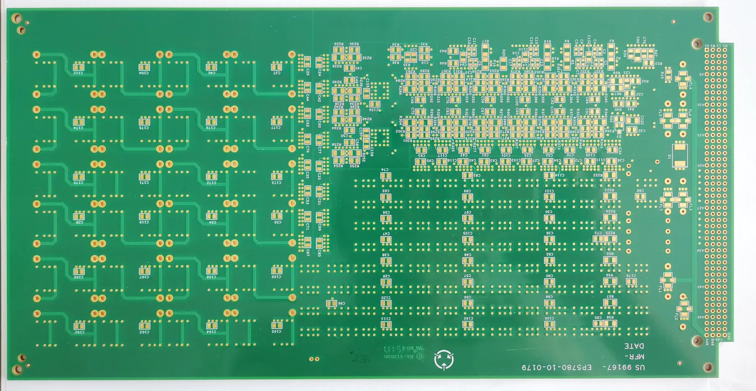
High frequency PCB
| P/N: S6l12760B0 | Layer Count: 6L | Min Line W/S: 5/5mil |
| Material: FR-4 Tg 135°C | Cu Thickness: 1/10z | Min PTH: 0.2mm |
| Board Thickness: 1. 6mm | Surface: ENIG+Gold Fingers | Application:Industry Control |
| Soldermask Color: Blue | Board Size: 167.64mmX126.75mm(1-up) | |
| Others: Min 3u" Au for ENIG Min 30u" Au for Gold Fingers | ||
Product Features
What is High-Frequency PCB
High-frequency PCBs generally provide a frequency range of 500MHz to 2 GHz, which can meet the needs of high-speed PCB design, microwave, radiofrequency and mobile applications. When the frequency is higher than 1 GHz, we can define it as high frequency.
Today, the complexity of electronic components and switches keeps increasing, and a faster signal flow is required than usual. Therefore, a higher transmission frequency is required. When integrating special signal requirements into electronic components and products, high-frequency PCB has many advantages, such as high efficiency, fast speed, low attenuation, and constant dielectric constant.
High-frequency PCB characteristics
1. DK should be small and stable, most of the time the smaller the better, the high DK may cause signal transmission delay.
2. DF should be small, whose size mainly affects the quality of signal transmission. The smaller the DF, the less the signal loss.
3. The thermal expansion coefficient should be the same as the copper foil as much as possible because the difference will cause the copper foil to separate in the cold and heat changes.
4. The water absorption rate must be low. In a humid environment, a high water absorption rate will affect DK and DF.
5. Heat resistance, chemical resistance, impact resistance, and peel resistance must be good.
High-frequency PCB - special materials
Special materials are needed to realize the high frequency provided by this type of printed circuit board, Because any change of their permittivity may affect the impedance of the PCBs. Many PCB designers choose Rogers dielectric material because it has lower dielectric loss, lower signal loss, lower circuit manufacturing costs, and is more suitable for rapid turnaround prototype applications among other materials.
Products application

High-frequency PCB is a special circuit board with high electromagnetic frequency, and the high-frequency frequency is above 1GHz. High-frequency PCBs have very high requirements on physical properties, precision, and technical parameters, and are often used in radar, military equipment, aerospace and other fields. Normally, high frequency pcb material is Rogers, Teflon, Isola, Nanya, Shengyi etc brands.
First of all, let's take a look at what materials are used to make high-frequency PCBs? The performance of high-frequency boards in wireless or other high-frequency applications depends on the building materials. For many applications, dielectric properties can be improved by using laminated FR4 materials. When manufacturing high-frequency PCBs, commonly used boards include Rogers, ISOLA, Taconic, Panasonic, Taiyao and other boards.
The DK of high-frequency PCB should be small and stable, usually the smaller the better, high-frequency PCB will cause signal transmission delay. DF should be small, which mainly affects the signal transmission quality. A smaller DF can reduce the signal loss accordingly, and in a humid environment, the water absorption rate is low and the water absorption capacity is strong, which has an impact on DK and DF.
Industry information
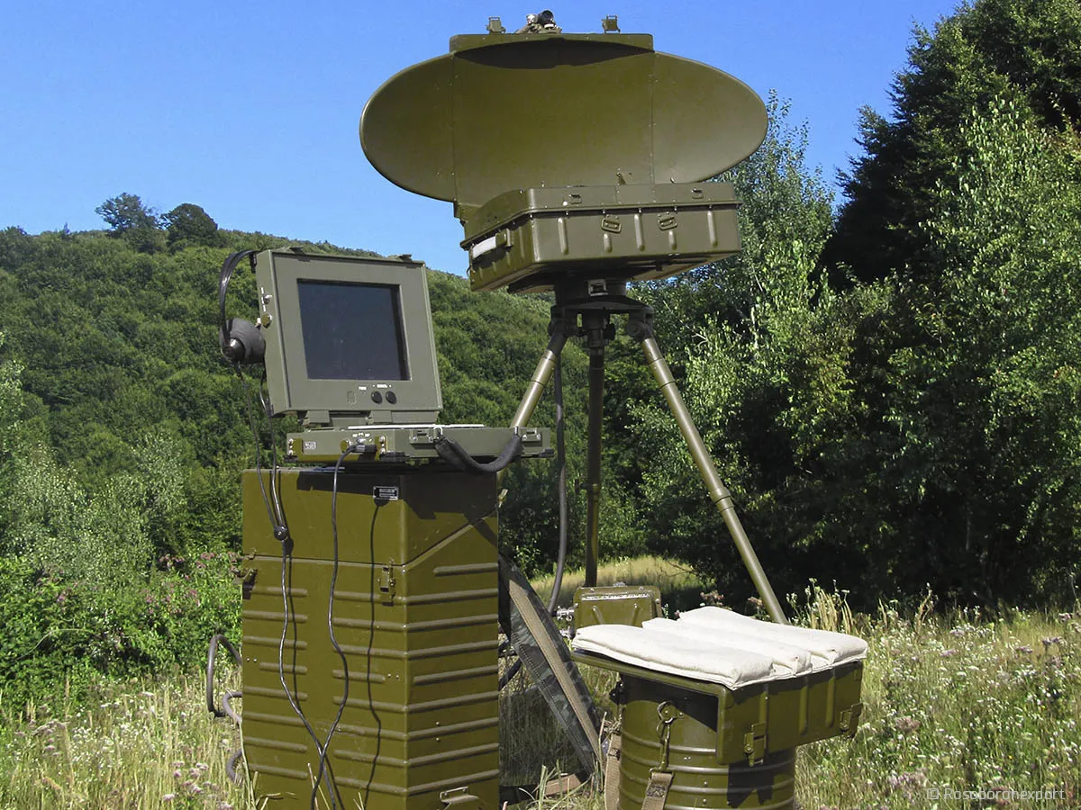
High frequency PCBs are generally used in radar systems, satellites, antennas, cellular telecommunications systems – power amplifiers and antennas, direct broadcast satellites, E-band point-to-point microwave links, radio frequency identification (RFID) tags, airborne and ground radar systems, millimeter wave applications, Missile guidance system, space satellite transceiver and other fields.
With the rapid development of science and technology, the functions of equipment are becoming more and more complex, and many equipment are designed in the microwave frequency band or even exceed the millimeter wave. This also means that the frequency continues to increase, and the requirements for the substrate of the circuit board are also getting higher and higher. As the frequency of the power signal increases, the loss of the base material is required to be very small, so the importance of high-frequency boards is highlighted.
Overview
What is Victory machining?
Victory machining is a manufacturing technique for removing material. It uses sharp cutting tools, available in a variety of shapes and sizes, which are precisely controlled by a computer. Victory stands for Computer Numerical Control.
How Victory machining works
Victory machining starts with a computer, on which designers prepare a part using CAD (Computer-aided Design) software. This digital part is then converted into a format that can be recognized by a Victory machine.
Instructions are sent to the Victory machine in the form of “G-Code” after which the machine can start cutting.
Most Victory machines have a “worktable” and work holding device to keep a block of material — known as the “workpiece” — in place. The worktable may or may not move, depending on the style of the machine.
When machining starts, the cutting tool makes contact with the workpiece, cutting away layers of material. The tool and/or workpiece is moved and/or rapidly rotated according to the G-Code instructions so that cuts are made in exactly the right places until the part is finished.
Different types of Victory machine
Victory machines include Victory mills, Victory turning machines (or lathes), Victory routers, and Electrical Discharge Machining (EDM) machines.
Victory mills have rotating cutting tools that are moved to different areas of the workpiece to make cuts and can be used to make many different pats. Victory lathes work the other way, rotating the workpiece against a stationary cutting tool, and are used to make cylindrical parts.
Victory routers are similar to Victory mills, but have less power and cannot cut the hardest materials. They can, however, be faster than Victory mills.
EDM uses electrical discharges (sparks) instead of a sharp cutting tool to cut material. No physical contact is made between the tool and the workpiece.
Victory machines are often defined by their number of axes. More axes mean they can move their tool and/or workpiece in a greater number of ways, giving greater cutting flexibility and the ability to make more complex parts in a shorter time.
What is a High Frequency PCB?
A High Frequency PCB is a specialized printed circuit board engineered to operate at high signal frequencies, typically above 1 GHz. These boards are designed to handle rapid signal transitions with minimal loss, making them essential for advanced electronics like telecommunications, radar systems, and high-speed computing. Unlike standard PCBs, they use unique materials and layouts to maintain signal integrity and reduce interference, ensuring reliable performance in cutting-edge applications.
How Are High Frequency PCBs Designed?
The design of a High Frequency PCB focuses on precision and signal optimization. Engineers use controlled impedance layouts to match the board’s electrical properties to the signals it carries. The structure includes smooth copper traces for low resistance, minimal vias to reduce signal disruption, and layered configurations to separate signals and ground planes. This careful planning ensures fast, clear data transmission critical for high-frequency operations.
How Does a High Frequency PCB Work?
A High Frequency PCB functions by transmitting rapid electrical signals through its conductive paths with minimal distortion. The board’s low dielectric materials keep signal speeds high, while its layout reduces electromagnetic interference (EMI). Ground planes shield signals from crosstalk, and the design ensures consistent impedance, allowing devices like antennas or processors to operate efficiently at microwave or radio frequencies.
Where Are High Frequency PCBs Used?
High Frequency PCBs power a range of modern electronics requiring fast signal processing. Key applications include:
- Telecommunications: Supports 5G networks and base stations.
- Aerospace: Drives radar and navigation systems.
- Medical: Enables high-speed imaging equipment.
- Computing: Boosts performance in servers and IoT devices.
Their ability to handle high-speed signals makes them vital in tech-driven industries.
Why Choose High Frequency PCBs?
High Frequency PCBs offer distinct advantages for specialized applications:
- Signal Clarity: Maintains data integrity at high speeds.
- Low Loss: Reduces energy dissipation for efficient operation.
- Compact Size: Supports dense layouts without sacrificing performance.
- EMI Reduction: Minimizes interference for reliable communication.
These benefits make them a top choice where precision and speed are non-negotiable.
What Materials Are Used in High Frequency PCBs?
High Frequency PCBs rely on advanced materials to perform at high speeds:
- Substrates: PTFE (Teflon) or ceramic-filled laminates for low dielectric loss.
- Copper: Smooth, high-purity copper for minimal signal resistance.
- Bonding Layers: Thermoset adhesives to maintain structural integrity.
These materials ensure fast signal travel and stability under high-frequency conditions.
How Do High Frequency PCBs Boost Signal Integrity?
High Frequency PCBs enhance signal integrity through smart design choices. Low-loss materials keep signal strength intact, while controlled impedance prevents reflections that distort data. Wide ground planes shield against noise, and precise trace spacing avoids crosstalk. This combination ensures clean, accurate signal transmission, crucial for devices operating at gigahertz frequencies.
How Are High Frequency PCBs Manufactured?
The manufacturing process for High Frequency PCBs is a careful sequence:
- Material Selection: Choose low-loss substrates like PTFE.
- Circuit Design: Plan impedance-controlled layouts.
- Etching: Use precision tools to form smooth copper traces.
- Lamination: Bond layers with heat and pressure.
- Inspection: Verify tolerances and signal paths.
This process ensures boards meet the exacting demands of high-frequency use.
How Are High Frequency PCBs Tested?
Testing High Frequency PCBs ensures they meet performance standards:
- Impedance Testing: Checks for consistent signal paths.
- Signal Loss: Measures dielectric and conductor losses.
- Environmental Stress: Tests durability under heat and humidity.
- EMI Scans: Confirms low interference levels.
These rigorous tests guarantee reliability in high-speed applications.
Why Are High Frequency PCBs Key in RF Systems?
In RF (Radio Frequency) communication systems, High Frequency PCBs are critical for their ability to manage rapid signals. They support antennas, transceivers, and amplifiers in devices like cell towers and satellites, delivering low signal loss and high precision. Their design minimizes noise and maintains signal strength, making them indispensable for seamless wireless connectivity.
FAQ
Reviews